投稿者: ryuji

  • 連載 #0 ドラゴンレーダーを真面目に作る

    何を作るか

    ドラゴンボールに出てくる「ドラゴンレーダー」を、現代の UWB (Ultra-Wide Band) 測距技術で本当に動くハードウェアとして作る

    具体的に:

    • プレイヤーが持つ円形 LCD 端末に、周囲のドラゴンボールが距離と方向と共に表示される
    • ドラゴンボール側は小型タグ (UWB トランスポンダ) で、複数個 (理想は 7 個) を会場に散らせる
    • LCD は玩具版ドラゴンレーダー (1980 年代バンダイ) の画面をオマージュした緑グリッド + コーラル三角ポインタ + ゴールド光点
    • 押せばボタン音、近づけば効果音 (SE)、見つけたら BGM

    これを DigiKey Make ONE Challenge 2026 (応募締切 2026-06-22) に出展、その後 9 月の Maker Faire Tokyo にデモ持ち込みする計画で動いている。

    なぜ UWB か

    ドラゴンレーダー作品は過去にもファンメイドで何度か試みられているが、ほぼ全て GPSBLE RSSI画像認識 ベースで作られていて、

    • GPS は屋内で精度が出ない、しかも数 m 単位の誤差
    • BLE RSSI は壁 1 枚で値が乱れる、向き判定不可
    • 画像認識はカメラ視野内しか見えない、隠されたら終わり

    5 cm 精度で距離が分かる、向きも 1〜2° で分かる、見通し外でも壁 1 枚なら抜ける」という条件を満たすのは UWB が唯一の現実解。スマホ (iPhone 11 以降、Pixel 6 Pro 等) にも入っている技術で、AirTag が「家具の裏のものを正確に指し示す」のはこれ。

    ハード的には NXP の SR150 (ホスト + AoA 対応) と SR040 (タグ専用、超低消費電力) を採用する。Murata から評価ボード (Type 2BP / Type 2DK) が出ていて、国内技適も取られている。

    なぜバンダイ風 UI か

    「Apple Find My っぽい現代的な UI」も検討したが、面白くない。

    ドラゴンレーダーは 1984 年に玩具として実物が存在する (バンダイ商品)。緑の LCD に緑のドット、ゴールドの数字、コーラル色の三角ポインタ、円形フィルムを回すスイープ。子供だった世代が大人になった今でも、この画面を見せると「あっ」となる

    技術が当時のフィクションに追いついた瞬間を、当時のビジュアル言語のまま届ける。これが本作品のテーゼ。

    構成の全体像

    [ プレイヤー手持ち端末 ]
      ESP32-P4 (RISC-V 400MHz, PSRAM 32MB)
        + 800x800 円形 IPS LCD (Waveshare 3.4C)
        + LVGL 9 (Bandai 風レーダー UI)
        + microSD (BGM/SE/ボイス)
        + I2S Codec ES8311 + スピーカー
        +─[UART 3Mbps 有線]─ Type 2BP EVK (QN9090 + SR150 UWB)
    
                                        ↕ UWB 6.5GHz (Ch5/9)
    
    [ ドラゴンボール (タグ) × 7 個 ]
      Type 2DK EVK (QN9090 + SR040 UWB)
        + 樹脂筐体 (3D プリント、内側に光ファイバー散らし)
        + 単 4 電池 × 2

    ESP32-P4 と Type 2BP は 物理 UART で直接配線する。WiFi / BLE は技適まわりの判断から使わない。

    工程と現状

    Phase 内容 状態
    0 部品入手、SDK 入手、開発環境構築
    1 ESP32-P4 上で LCD + Bandai UI が動く (ダミーデータ)
    2a NXP UWBIOT SDK の MCUXpresso ヘッドレスビルド検証
    2b QN9090 ファーム改造で UWB ranging 結果を ASCII で吐かせる
    2c 改造ファームを焼いて、UART 3Mbps で距離 + 方位が流れることを実機確認
    2d ESP32-P4 ↔ Type 2BP の物理 UART 配線 + LVGL に実データ反映 進行中
    3 ドラゴンボール側 (Type 2DK) のタグ化 ファーム + 筐体 これから
    4 音声 / 効果音 / BGM これから
    5 全体筐体 CAD + 組立 これから

    開発開始は 2026-04-29、応募締切は 2026-06-22。今のところスケジュールに 1 週間以上の余裕がある。

    なぜここに書くか

    この作品は趣味として作るが、過程で得た技術知見 (UWB / NXP UWBIOT SDK / ESP-IDF / LVGL / 組込ハード設計 / 技適) は 同じことをやろうとする人にも役に立つはず。なので進行中の発見を分割して記事にしていく。

    最初に切り出すのは以下:

    1. dk6prog で QN9090 を USB ISP だけで焼く ← SWD ハード無しでもファーム書ける話
    2. MCUXpresso headless build でファームを 10 秒で回す ← IDE を立ち上げずにビルド
    3. UWB ranging が動かない原因は UCI 世代差だった ← 異種 UWB チップを組ませる時のハマりどころ
    4. ESP32-P4 × LVGL で Bandai ドラゴンレーダー UI を作る ← 玩具っぽい温かみある UI を LVGL で
    5. 技適未確認ボードをコンテストで使うなら ← 国内出展のための設計判断

    本作品の進捗は完成までこのブログで時系列に記録する。完成しなかったらそれもまた記録として残す。

    期待値の調整

    「ドラゴンレーダーが動く」とは何か、最初に明確にしておく:

    • ✅ 5 cm 程度の距離精度で近くにあるボールの距離が分かる
    • ✅ AoA でボールの方向 (左右) が分かる (前後判定は補助的)
    • ✅ 7 個まで同時表示できる (round-robin で測距)
    • ❌ 壁を貫通する透視能力は無い (UWB は壁 2 枚以上で減衰する)
    • ❌ 「ピッピッ」音は出るが、原作のサーチ音とは違う (著作権)

    現代の物理法則の上で実装可能な範囲で最大限フィクションに近づける、それが本作品の制約。

    完成記事 (動作デモ動画 + 全工程まとめ) は 6/22 直前に公開予定。それまでは過程の知見を順次共有する。

  • 技適未確認の WiFi ボードを国内コンテストに出すなら何を捨てるか

    要約

    中国メーカーから個人輸入した ESP32 系ボード (含む WiFi6 モジュール) を、国内のメイカーコンテストに展示することを考えるとき、最初にチェックすべきは「そのボード上の無線モジュールに技適マークがあるか」。

    技適マーク (Telec) は電波法に基づく型式認定で、これ無しの無線機を電波を出す状態で国内使用すると電波法違反になる。特例制度 (180 日試験運用) はあるが、公開イベント常時運用には合わない

    技適未確認ボードを「使うかどうか」を悩むのではなく、技適なしを前提にハードウェアアーキテクチャを設計し直すのが正しい意思決定。本記事ではその意思決定を最近実例ベースで整理する。

    何が問題なのか

    ESP32 系ボード、特に 「ESP32-P4 + ESP32-C6 (WiFi6 コンパニオン)」を組み合わせた製品は、Espressif 単体モジュールでは技適済の variant があるが、第三者メーカーが基板に載せて組み立てた完成品は技適マーク (基板上のシールド表面に R 003-XXXXXX の刻印) がそのまま継承されないことが多い。

    具体例:

    • Espressif の ESP32-C6-WROOM-1 モジュールには技適済 SKU が存在する
    • ところが Waveshare 系の「ESP32-P4-WIFI6-Touch-LCD-XC」のような完成品ボードに載っている ESP32-C6 が、技適済 SKU を使っているとは限らない
    • ボード上のシールドに R 番号が刻印されているか目視確認するしか手段がない

    筆者の手元の Waveshare ESP32-P4-WIFI6-Touch-LCD-3.4C は 目視で技適マーク確認できずだった。

    電波法の建付け

    総務省の電波法では、技適マーク (技術基準適合証明、特定無線設備の技術基準適合認定) 未取得の無線設備を国内で電波を発射する状態で使用すると違反となる (第 4 条 / 第 38 条系)。

    ただし救済として 電波法第 4 条の 2 に基づく「実験等無線局」/「特例制度」 があり、開発・実験目的に限り 180 日間届出ベースで使用できる枠が用意されている。

    ただし これは「自宅・自社の閉じた環境で開発する」想定の制度で、

    • 公開イベント (Maker Faire、コンテスト出展、商業展示) で「常時動いている」状態は実験運用とみなされにくい
    • 違反扱いになると刑事罰 (1 年以下の懲役または 100 万円以下の罰金) の可能性がある
    • 主催者側 (大型イベントは大概スタッフが電波法を理解している) から会場ルールでも止められる

    「コンテストに出す」という目的なら、特例制度を当てにせず WiFi/BT を最初から使わない設計にするのが現実解。

    設計上の意思決定

    筆者の場合は ESP32-P4 系ボードを LCD ホストとして使う前提があり、「ボード上の WiFi/BT を一切初期化せず、有線通信に切り替える」設計を採用した。

    具体的に何を犠牲にして何を残したか:

    機能 当初の構想 技適なし前提後
    無線測距 (UWB) UWB チップ (Murata SR150/SR040) で実装 同じ (UWB は別途技適済モジュールを使用)
    デバッグログ転送 WiFi で開発端末に飛ばす USB シリアルのみ
    センサノードとの通信 BLE / WiFi で散発接続 物理 UART 配線
    OTA ファーム更新 WiFi 経由 SD カード差し替え / USB
    Web 設定 UI スマホブラウザから WiFi 経由 LCD タッチ UI のみ

    物理配線で全部やる」と決めると、設計はむしろシンプルになる。ペアリング・認証・電波輻射の干渉考慮が消える。

    チェックリスト: 自分のボードで何を確認すべきか

    国内コンテスト用に中華製評価ボードを選ぶときは以下を順に:

    1. 基板上の無線モジュール (銀色シールド) 表面に技適マーク or R 003-XXXXXX の刻印があるか目視
    2. メーカー商品ページに「Japan / 技適 / Japanese certification」明示があるか
    3. 国内代理店経由なら、その代理店が技適済バージョンとして売っているか
    4. どれもダメなら → そのボードの WiFi/BT は使わない設計にするか、技適済の別ボード (ESP32-DevKitC-32E など) に置き換える

    技適済 ESP32 系の入手:

    • 国内代理店 (秋月電子、スイッチサイエンス、マルツ等) から正規流通品を買えば技適マーク済 (R 003-XXXXXX 刻印あり)
    • AliExpress / Taobao から個人輸入したものは大概グレー

    まとめ

    • 公開イベント展示が前提なら、WiFi/BT を使う設計を最初から避けるのが安全
    • 技適マークの有無は ボード本体ではなく、基板上の無線モジュールのシールドに刻印されているかで判断
    • ハードウェア構成を「技適なしを前提に再設計」する方が、特例制度を当てにするより早くて確実
    • 開発生産性的にも、有線通信に絞ると ペアリング・認証・電波干渉が消えてシンプルになることが多い

    最近の組込デバイスは「WiFi/BT が付いてるのがデフォルト」になっていて、それを使わない設計を最初から組むのは少し勇気がいるが、コンテスト出展という目的を考えると、技適まわりは設計上の制約ではなく前提として扱うべき項目。

    電波法は古い法律だが、まだ生きている。

  • ESP32-P4 × LVGL で「バンダイ ドラゴンレーダー」風 UI を本気で再現する

    要約

    ESP32-P4 + 800×800 円形 LCD (Waveshare 3.4C / IPS) という贅沢なハードで、1980 年代バンダイから出ていた玩具版「ドラゴンレーダー」の画面表示を再現してみた記録。

    ポイントは 4 つ:

    1. ── 緑 CRT 背景 + 太い黒グリッド + ゴールド数字 + コーラル三角ポインタ
    2. 三角ポインタ ── 「現在地」を表す塗り潰し三角を LVGL の lv_obj 矩形スタックで描く (LVGL 9 にはネイティブの三角プリミティブが無いため)
    3. スイープ ── 円弧 30 度幅の lv_arc を回し続ける
    4. 光点 (ドラゴンボール) ── 距離→対数スケール、AoA 方位→極座標変換で配置

    LVGL は工業 HMI に最適化されていて「アニメ・玩具風の温かみある画面」を作るのが意外と難しい。本記事はその難易度をどう越えたかの記録。

    ハードと前提

    • MCU: ESP32-P4 (RISC-V dual-core 400MHz、PSRAM 32MB)
    • LCD: 800×800 round IPS (Waveshare 3.4C)
    • フレームワーク: ESP-IDF v5.5.4、LVGL 9.5.0、esp_lvgl_adapter 経由
    • 描画モード: triple partial buffer + tear-avoid

    LCD は MIPI-DSI で繋がっていて、フレームバッファは PSRAM に乗る。Waveshare BSP (waveshare/esp32_p4_wifi6_touch_lcd_xc) を managed component で取り込めば LVGL までの配線は数行で済む。

    カラーパレット

    玩具版の写真を観察してパレットを取った:

    // theme.h
    #define DR_COLOR_BG       lv_color_hex(0x2A9040)  // 緑 CRT
    #define DR_COLOR_GRID     lv_color_hex(0x001008)  // ほぼ黒
    #define DR_COLOR_SWEEP    lv_color_hex(0xA0FFB0)  // スイープのトレイル
    #define DR_COLOR_TEXT     lv_color_hex(0xFFD700)  // ゴールド (数字 / ラベル)
    #define DR_COLOR_DOT      lv_color_hex(0xFFC800)  // ドラゴンボール (オレンジゴールド)
    #define DR_COLOR_POINTER  lv_color_hex(0xFF6E50)  // コーラル (中央三角)

    ポイントは 背景の緑をくすませる こと。サチった #00FF00 を使うと「LED マトリクス」っぽくなり玩具感が消える。 #2A9040 くらいのやや暗くて青みのある緑が CRT 蛍光体っぽくて良い。

    グリッド

    LVGL の標準では「画面全体に等間隔の格子線」を引くプリミティブは無いので lv_line_create を縦横ループで配置する。

    #define GRID_STEP 50
    for (int x = GRID_STEP; x < DR_SCREEN_SIZE; x += GRID_STEP) {
        static lv_point_precise_t pts[20][2];
        int i = x / GRID_STEP - 1;
        pts[i][0].x = x; pts[i][0].y = 0;
        pts[i][1].x = x; pts[i][1].y = DR_SCREEN_SIZE;
        lv_obj_t *line = lv_line_create(parent);
        lv_line_set_points(line, pts[i], 2);
        lv_obj_set_style_line_color(line, DR_COLOR_GRID, 0);
        lv_obj_set_style_line_width(line, 2, 0);
        lv_obj_set_style_line_opa(line, LV_OPA_80, 0);
    }

    lv_point_precise_tstatic にしないと描画タイミングでスタック上のメモリが消えて画面に変な線が現れる。LVGL のプリミティブはポインタを保持するだけで、内部コピーしないことが多いので注意。

    三角ポインタ ── 一番苦戦したパーツ

    LVGL 9 に 塗り潰し三角プリミティブは無いlv_canvas で自前描画してもいいが、800×800 のフルキャンバスを PSRAM に保持するのは重い。

    そこで採用したのが 水平スキャンラインで矩形を積む方式:

    #define PT_SIZE 16     // 三角の半幅
    #define PT_STEP 2      // スキャンラインの厚さ
    const int y_top    = DR_CENTER - PT_SIZE;
    const int y_bottom = DR_CENTER + PT_SIZE / 2;
    const int height   = y_bottom - y_top;
    
    for (int y = y_top; y <= y_bottom; y += PT_STEP) {
        int dy = y - y_top;
        int half_w = (dy * PT_SIZE) / height;
        if (half_w < 1) half_w = 1;
    
        lv_obj_t *seg = lv_obj_create(parent);
        lv_obj_remove_style_all(seg);
        lv_obj_set_size(seg, half_w * 2, PT_STEP);
        lv_obj_set_pos(seg, DR_CENTER - half_w, y);
        lv_obj_set_style_bg_color(seg, DR_COLOR_POINTER, 0);
        lv_obj_set_style_bg_opa(seg, LV_OPA_COVER, 0);
    }

    頂点が上、底辺が下の塗り潰し三角を、PT_STEP=2 ピクセル幅の矩形を ~12 個積んで再現する。メモリは矩形 12 個分しか食わない (内部的に lv_obj は数百バイト)。LVGL の合成エンジンが矩形描画はべらぼうに速いので描画コストもタダ同然。

    回転させたい場合は lv_obj_set_style_transform_angle でグループ全体を回せばよい。三角ポインタを「機体の向きに合わせて回転」させる用途にも使える。

    スイープアーク

    円弧を回すのは LVGL のお家芸:

    lv_obj_t *arc = lv_arc_create(parent);
    lv_obj_set_size(arc, DR_RADAR_RING_R2 * 2, DR_RADAR_RING_R2 * 2);
    lv_obj_align(arc, LV_ALIGN_CENTER, 0, 0);
    lv_arc_set_bg_angles(arc, 0, 360);
    lv_arc_set_rotation(arc, 270);
    lv_arc_set_angles(arc, 0, 30);  // 30 度幅
    lv_obj_set_style_arc_color(arc, DR_COLOR_SWEEP, LV_PART_INDICATOR);
    lv_obj_set_style_arc_width(arc, DR_RADAR_RING_R2, LV_PART_INDICATOR);
    lv_obj_set_style_arc_opa(arc, LV_OPA_30, LV_PART_INDICATOR);
    
    lv_anim_t a;
    lv_anim_init(&a);
    lv_anim_set_var(&a, arc);
    lv_anim_set_exec_cb(&a, (lv_anim_exec_xcb_t)lv_arc_set_rotation);
    lv_anim_set_values(&a, 270, 270 + 360);
    lv_anim_set_duration(&a, 1500);
    lv_anim_set_repeat_count(&a, LV_ANIM_REPEAT_INFINITE);
    lv_anim_start(&a);

    arc_width = R2 (リング全径) にして、塗り部分の不透明度を 30% に落とすと「スポットライトが回転する」風になる。トレイル感を出したいなら 2 本目のアークを反対側に置いて opa=10% にする手もある。

    光点 (ドラゴンボール) 配置

    UWB ranging から流れてくる distance_mmazimuth_deg を画面座標に変換する:

    static int32_t distance_to_radius_px(uint16_t distance_mm) {
        if (distance_mm == 0) return 0;
        if (distance_mm >= DR_RANGE_MAX_MM) return DR_RADAR_RING_R2;
        float ratio = logf(1.0f + (float)distance_mm / 1000.0f)
                    / logf(1.0f + (float)DR_RANGE_MAX_MM / 1000.0f);
        return (int32_t)(DR_RADAR_RING_R2 * ratio);
    }
    
    static void polar_to_cartesian(uint16_t distance_mm, int16_t azimuth_deg,
                                   int32_t *x, int32_t *y) {
        int32_t r = distance_to_radius_px(distance_mm);
        float az_rad = azimuth_deg * M_PI / 180.0f;
        *x = DR_CENTER + (int32_t)(r * sinf(az_rad));
        *y = DR_CENTER - (int32_t)(r * cosf(az_rad));
    }

    距離 → 半径は 対数スケールにする。線形だと「近い時は中心にくっつく、遠い時はリングの端に張り付く」となるが、人間の空間感覚に合うのは対数。1m での解像度を大きく取り、10m の精度を犠牲にする。

    光点本体は丸オブジェクトに シャドウで発光感を出す:

    lv_obj_t *dot = lv_obj_create(parent);
    lv_obj_set_size(dot, 30, 30);
    lv_obj_set_style_radius(dot, LV_RADIUS_CIRCLE, 0);
    lv_obj_set_style_bg_color(dot, DR_COLOR_DOT, 0);
    lv_obj_set_style_shadow_color(dot, DR_COLOR_DOT, 0);
    lv_obj_set_style_shadow_width(dot, 28, 0);
    lv_obj_set_style_shadow_opa(dot, LV_OPA_70, 0);

    shadow_width = 28 (本体径とほぼ同じ) で等方ハローができ、ドラゴンボールの「内側から光ってる」雰囲気が出る。

    ハマりどころメモ

    症状 原因 / 対処
    起動時にリンカが --enable-non-contiguous-regions discards section ... 21KB ESP32-P4 v1.x シリコンで CONFIG_SPIRAM_XIP_FROM_PSRAM 有効だと IRAM 溢れ → 無効化
    LCD が真っ黒 CONFIG_LV_USE_PERF_MONITOR=nCOMPILER_OPTIMIZATION_SIZE=y、L2 cache 128KB に落とす
    描画がカクつく LV_COLOR_DEPTH=16、frame buffer を PSRAM に置く、triple_partial モード
    緑がサチった LED 色になる パレットを #2A9040 系のくすんだ緑に。#00FF00 は使わない

    動かしてみた

    LCD のフォトを撮って横で玩具のドラゴンレーダーと比較した時、「電池入れて 30 年経った玩具」っぽい質感が出てしまった (緑が少しくすんでいる + 黒グリッドが太い + フォントがゴールド) ── 結果としてその”古色感”が逆に良かった。

    LVGL は HMI 用ライブラリだけど、プリミティブを工夫すれば「玩具・アニメ的な温かみのある UI」も十分作れる。三角プリミティブが無いから諦める前に、矩形スタックで作れないか考えてみる価値はある。

  • UWB ranging が動かない真犯人は「UCI 世代差」だった話

    要約

    異なる NXP UWB チップ (SR150 / SR040) を載せた 2 つの評価ボードを ranging させようとしたら、

    • 両者の RANGE_DATA_NTF (測距結果通知) に乗っている session ID が違って見える
    • 一方は 0x00000001、もう一方は 0x11223344

    「session ID が違うから pair しないんだ」と最初は誤診したが、SDK のソースを当たると 両方ともデフォルトで 0x11223344 を設定していることが判明。

    実際に違うのは UCI (UWB Command Interface) のプロトコル世代で、UCI v1.x は Session ID を payload にそのまま乗せるが、UCI v2.0 以降は Session Handle というラッパに置き換わる。通知フィールドが見た目同じバイト位置でも、解釈が違うので一致しない

    両方を UCI v1.31 世代の SDK に揃えた瞬間に ranging が成立した。誤診から本質に辿り着くまでの記録。

    環境

    • Initiator: NXP SR150 ベースの評価ボード (Murata Type 2BP EVK Rev 4.1)
    • Responder: NXP SR040 ベースの評価ボード (Murata Type 2DK EVK)
    • 両者にメーカープリビルド済の standalone ranging デモを焼いて、UART 経由で生の UCI トレースを観察

    最初の観測

    電源を入れて並べると、2 つの EVK はとりあえずお互いの存在は認識する (TX/RX が走る) のだが、ranging が完了しない。Murata 提供の Python テストスクリプトも distance を 1 度も print しないまま終わる。

    両方の UART を cat /dev/ttyUSB* で生キャプチャして UCI フレームを抜き出すと、

    • 2BP (SR150 / 新しい SDK) 側: NTF 内の session 識別フィールドが 01 00 00 00 (リトルエンディアン解釈で 0x00000001)
    • 2DK (SR040 / 古い SDK) 側: 同じ位置が 44 33 22 11 (リトルエンディアン解釈で 0x11223344)

    ぱっと見「2 つの session ID が違う、だから ranging が成立しない」と読みたくなる。これが間違いだった。

    SDK のソースを当たる

    それぞれの SDK のサンプルコードを grep -nrR SESSION_ID する。

    demos/SR1XX/demo_ranging_controller/demo_ranging_controller.c:
      #define RANGING_APP_SESSION_ID 0x11223344
    
    demos/SR040/demo_tracker_sr040/app_Ranging_Cfg.h:
      #define RANGING_APP_SESSION_ID 0x11223344

    両方とも 0x11223344 を設定している。つまりアプリケーション層で投げているセッション ID は一致しているはず。

    ということは、UART で見ている「session 識別フィールド」がそもそも別物を指している可能性が高い。

    UCI 仕様書を読み直す

    NXP の SR150 UCI Specification を当たると、v1.x と v2.0 で RANGE_DATA_NTF の最初の数バイトの定義が変わっている:

    バイト位置 UCI v1.x UCI v2.0
    0-3 Sequence Number Sequence Number
    4-7 Session ID (アプリが設定した 32-bit 値そのまま) Session Handle (UCI スタックが割り当てた識別子)
    8-11 Rcr Block Index Rcr Block Index

    v2.0 で導入された Session Handle は SDK 内部で SessionInit 時に動的に発行される (例: 0x00000001 から順に割り当てる) 識別子で、アプリが設定した Session ID とは別物。アプリ層 API では Session ID を渡すが、UCI バイナリ層では Handle に置き換わる。

    つまり、

    • SR150 + 新しい SDK: UCI v2.0 → NTF の 4-7 バイト目には Session Handle (0x00000001) が乗る
    • SR040 + 古い SDK: UCI v1.x → NTF の 4-7 バイト目には Session ID (0x11223344) がそのまま乗る

    両者は同じバイト位置に別の意味の値を入れていて、当然 ranging session の照合に失敗する。「session ID が違う」のではなく「session 識別の規約が違う」が本質だった。

    揃え方

    選択肢は 2 つ:

    1. SR040 側の SDK を v2.0 世代に上げる
    2. SR150 側の SDK を v1.x 世代に下げる

    SR040 はメーカー (Murata) が校正済の standalone バイナリを v1.x 世代でしか出してくれていなかったので、現実解は (2)。SR150 側を NXP UWBIOT SDK v04.04.03 (UCI v1.31) の bare バイナリに差し替え、両者の UCI 世代を v1.31 に統一した。

    結果: 焼き直して電源入れた瞬間、UART に TWR[0].distance : 26 のような distance 値が湯水のように流れ始めた。20 秒で 200+ サンプル、distance は両端で平均 0.5cm 以内に一致 (DS-TWR が正しく完走している証拠)。

    教訓

    • 「session ID が違う」のように『見える』状態を素直に取らない。NTF のバイト位置と UCI 仕様書の世代を必ず照合する
    • 異種チップを組ませる時は UCI 仕様の世代揃えが必須。SR150 と SR040 は同じ NXP 製でも世代が異なる SDK で出てくる
    • デバッグの第 1 歩は SDK ソースの grep。「定数として何を設定しているか」を直接確認すれば、UART で観測した値との差分が見える

    UCI が業界標準 (FiRa Consortium 仕様) になりつつあるとはいえ、世代差を吸収するレイヤはまだ薄い。UWB を触る時は両端の SDK バージョンを意識して揃えることが、ranging を素直に動かす近道。

  • MCUXpresso IDE の headless build で組込ファームを 10 秒で回す

    要約

    NXP が出している MCUXpresso IDE は Eclipse CDT ベースなので、見た目は GUI でも中身は コマンドラインから単独でビルドを叩ける

    mcuxpressoide -application org.eclipse.cdt.managedbuilder.core.headlessbuild という呪文を覚えてしまえば、IDE を立ち上げる時間も、Eclipse のウィンドウマネージャ周りで詰まる時間もゼロにできて、1 回 9 秒 でビルドが回るようになる。

    「IDE で開いて、メニューから Build をクリックして、終わるのを待って」というループを 10 倍速くしたい人向けの記事。

    なぜ GUI で回すと遅いか

    NXP UWBIOT SDK のようなボリュームある SDK を MCUXpresso GUI で開くと、

    1. ワークスペースを開くだけで 30 秒以上
    2. インデックス再構築で CPU 100% が 2〜3 分
    3. Build のたびに「Project Indexer Update」が走り直して数十秒

    ソースを 1 行直して焼き直したいだけなのに毎回これに付き合うのは消耗する。

    Eclipse CDT は元々 IBM (JDT) から派生した CDT 部分でヘッドレスビルダを持っていて、-application org.eclipse.cdt.managedbuilder.core.headlessbuild を渡せば IDE の UI を起動せずに同じツールチェーンで .project / .cproject をビルドできる

    環境

    • Ubuntu 24.04
    • MCUXpresso IDE for Linux (/usr/local/mcuxpressoide-25.6.136/ide/)
    • 内蔵 JRE (OpenJDK 17) と内蔵 arm-none-eabi-gcc を使う

    ヘッドレスビルド呪文

    xvfb-run --auto-servernum --server-args="-screen 0 1024x768x24" \
      /usr/local/mcuxpressoide-25.6.136/ide/mcuxpressoide \
      -nosplash \
      -application org.eclipse.cdt.managedbuilder.core.headlessbuild \
      -data /tmp/mcux-ws \
      -import /path/to/project/MyProject \
      -cleanBuild "MyProject/Debug"

    各オプションの意味:

    オプション 意味
    xvfb-run Linux サーバや CI で X が無くても Eclipse の GTK 依存を満たす仮想ディスプレイを立てる
    -nosplash スプラッシュ画面を出さない (ヘッドレスでは不要)
    -application <id> Eclipse プラットフォームの起動アプリケーションを指定。CDT のヘッドレスビルダはこの ID
    -data <dir> Eclipse ワークスペース。事前に存在しなくても自動作成される
    -import <project> .project のあるディレクトリ。プロジェクト名はその中身から読み取られる
    -cleanBuild "Project/Config" クリーンビルドする対象を「プロジェクト名/ビルドコンフィグ名」で指定

    ポイントは Project/Config がプロジェクト内の .cproject に書かれている名前と完全一致しないとダメ という所。GUI で右クリック → Properties → C/C++ Build → 設定タブのリスト名と一致する。

    .cproject ファイル内で:

    <configuration name="Debug" ...>
    <configuration name="Release" ...>

    これを grep するのが手っ取り早い。

    結果

    筆者のケース (NXP UWBIOT SDK v04.04.03 + Murata Type 2BP 向け demo_ranging_controller) では:

    [1/12] Performing build step for 'bootloader'
    ...
    [10/12] Linking CXX executable RhodesV4_SE.axf
    Memory region         Used Size  Region Size  %age Used
       PROGRAM_FLASH:      353180 B     629471 B     56.11%
                SRAM:       32576 B        87 KB     36.57%
               SRAM1:         45 KB        64 KB     70.31%
    [11/12] Generating binary image
    ...
    Build Finished. 0 errors, 1 warnings. (took 9s.620ms)

    9.6 秒で .axf + .bin まで生成される。GUI で開きっぱなしより速い (差分ビルドなら GUI でも数秒だが、起動時間を含めると勝てない)。

    おまけ: シェル関数化

    毎回タイプするのは流石に辛いので zshrc / bashrc に入れておく:

    mcux_build() {
      local proj="$1"
      local cfg="${2:-Debug}"
      xvfb-run --auto-servernum --server-args="-screen 0 1024x768x24" \
        /usr/local/mcuxpressoide-25.6.136/ide/mcuxpressoide \
        -nosplash \
        -application org.eclipse.cdt.managedbuilder.core.headlessbuild \
        -data /tmp/mcux-ws \
        -import "$proj" \
        -cleanBuild "$(basename "$proj")/$cfg"
    }
    
    # 使う側
    mcux_build /path/to/MyProject Debug

    これで mcux_build . のような短い呼び出しで CI でも開発でも使える。

    ハマりどころメモ

    症状 原因 / 対処
    No projects matched -cleanBuild の引数が .cproject のコンフィグ名と一致してない
    DISPLAY 環境変数が設定されてない xvfb-run を使う、もしくは X 転送 (ssh -X)
    Workspace not initialized -data で指定したパスのパーミッションが書込み不可。/tmp/ 以下が無難
    ビルドが空のサイレント終了 -import のパスが間違っているとログも吐かず終わることがある。絶対パス推奨

    何が良くなったか

    • 編集 → ビルド → 焼き のループが体感 1 桁速くなる
    • CI で組込ファームをビルド できる。Pull Request ごとにファームのバイナリ差分を取れる
    • IDE GUI のメモリ食いが消えるので、開発端末のリソースを LLM チャットや別 IDE に回せる

    NXP に限らず Eclipse CDT ベースの組込 IDE (STM32CubeIDE 等) は同じ仕組みで動く。「IDE を立ち上げてビルドする」習慣をやめると、組込開発の生産性は素直に上がる

  • dk6prog (SPSDK) で QN9090 を USB ISP だけで焼く

    要約

    NXP QN9090 を載せた評価ボード (Murata Type 2BP EVK / 2DK EVK 等) のファームを書き換えるとき、SWD (J-Link / MCU-Link Pro) が標準ルートとされるが、ボードのデバッグピンが折れていたり配線できない事情があるとそこで詰まる。

    そこで便利なのが SPSDK に含まれる dk6prog という Python ツールで、USB ケーブル 1 本だけで ISP (In-System Programming) モードに入って書き換えできる。

    本記事では Linux 上で pip install spsdk だけで導入して、QN9090 のフラッシュ全領域を吸い出してバックアップ → カスタムファームを書き込む手順を 1 枚にまとめる。

    なぜこれが効くか

    QN9090 (および兄弟の DK6 シリーズ) は ROM ブートローダに ISP モードを備えていて、特定ピン (PIO_5 / ISP_ENTRY) を引いた状態でリセットすると UART 経由でフラッシュ操作を受け付ける。Murata / NXP の DK6 EVK はオンボードに FTDI FT230X USB-UART ブリッジが載っていて、USB ケーブル 1 本でこの UART に到達できる。

    SWD で書ける環境を持っていない人 (J-Link を持っていない、MCU-Link Pro が手元にない、開発端末が Windows 縛りで動かないなど) でも、Python が動けば書けるのが大きい。

    手順

    0. 前提

    • 開発端末: Ubuntu 24.04 (Linux 一般、macOS でも同様)
    • ターゲット: NXP QN9090 ベースの DK6 EVK (例: Murata Type 2BP / 2DK)
    • USB ケーブル (データ通信対応 micro-USB、充電専用品はダメ)

    1. SPSDK をインストール

    pip install spsdk pyftdi

    (venv 推奨。SPSDK は依存が多めなので素の Python に入れると他プロジェクトと衝突しやすい。)

    2. USB 接続して認識を確認

    EVK と PC を USB でつないだ状態で:

    dk6prog listdev
    List of available devices:
    DEVICE ID: DM86TTWC, VID: 0x403, PID: 0x6015, ...

    DEVICE ID がそのまま -d の引数になる。Murata 出荷品は全 EVK で同じシリアルが振られていることがあり、複数挿していると後続コマンドで衝突するので、作業時は対象 1 個だけ挿す

    3. ISP モードに入れて疎通確認

    EVK の ISP ボタン (PIO_5 / ISP_ENTRY) を押しながら RESET を離すと ISP モードに入る (ボードによっては「ISP」シルク印刷がある専用ボタン、ない場合は基板上のテストパッドを GND に落とす)。

    dk6prog -d DM86TTWC info
    Chip ID: 0x88888888
    ROM Version: 0x140000cc
    
      Memory   Memory ID   Base Address   Length    Sector Size
    ----------------------------------------------------------------
      FLASH    0           0x0            0x9de00   0x200
      PSECT    1           0x0            0x1e0     0x10
      ...

    info が返ってくれば疎通 OK。

    4. 焼く前に「出荷時 FW」をバックアップする

    これが本記事で一番伝えたい部分。Murata の EVK は出荷時にメーカー校正済の FW が入っており、これを潰すと TX パワーや水晶発振の校正が失われる。

    dk6prog -d DM86TTWC read 0 0x9DE00 -o factory_backup.bin

    0x9DE00 (約 632KB) が FLASH 全長。1 度だけ取って、git に上げる代わりに「火事から助かる」場所に保管しておくと心理的に強い。

    5. カスタムファームを書き込む

    dk6prog -d DM86TTWC erase 0 0x9DE00
    dk6prog -d DM86TTWC write 0 my_custom_fw.bin

    (erase は write の中で勝手にやってくれる版もあるが、明示的に erase してから write する方が事故が少ない。)

    6. 復旧したいとき

    dk6prog -d DM86TTWC erase 0 0x9DE00
    dk6prog -d DM86TTWC write 0 factory_backup.bin

    これで step 0 の状態に戻る。安心。

    ハマりどころメモ

    症状 原因 / 回避
    2 USB devices match URL 同じシリアルの EVK が複数挿さっている。物理的に片方を抜く
    no langid permission issue pyftdi backend は libusb で root 権限要求することがある → sudo -E で実行 (環境変数を保持しないと PATH が消えるので -E 必須)
    Failed to enter ISP mode ISP ボタン押しが遅い / 早い。USB を抜いてボタン押しっぱなしで挿し直す → リセットボタンも併用
    Chip ID: 0x88888888 のまま これは正常 (ISP モードで MAC アドレスが返らない仕様)

    何が良くなったか

    • SWD ハードが要らない (J-Link / MCU-Link Pro は 1 台 1〜2 万円)
    • OS を選ばない (Windows 限定の DK6Programmer.exe に縛られない)
    • CI に組み込める (シェルから叩けるので、ビルド → 焼き → テスト を一筆書きできる)

    「SWD ピンが曲がってた」「IDE のドライバが入らない」みたいな ハードウェアやアーキテクチャに本質的でない問題で停滞している人にとって、dk6prog 経由のフラッシュは数時間〜数日を取り戻すポテンシャルがある。

    参考

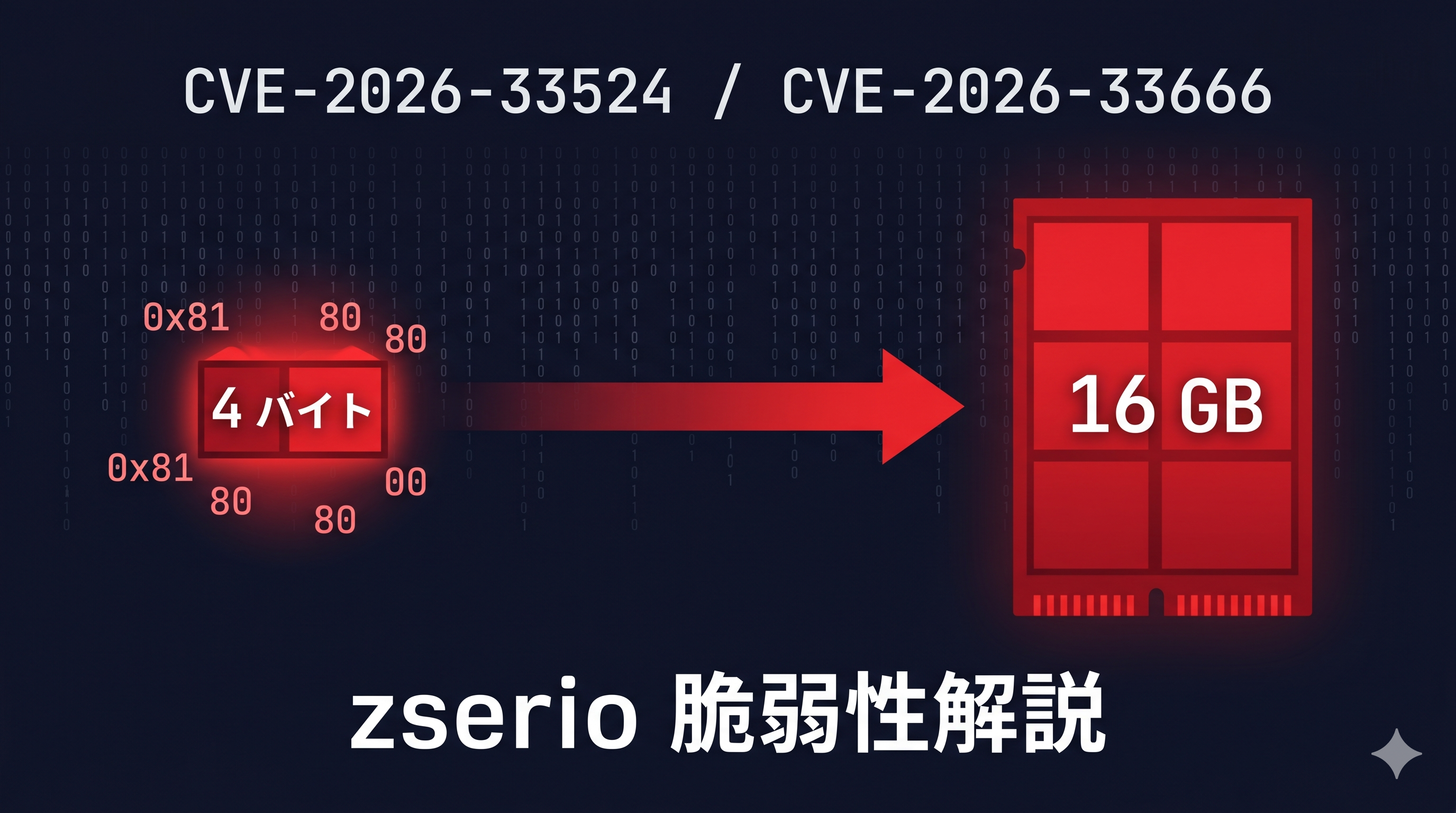
  • 全世界の車で動く地図ソフトウェアに、たった 4 バイトで攻撃できる脆弱性が見つかりました ── CVE-2026-33524 / CVE-2026-33666

    全世界の車で動く地図ソフトウェアに、たった 4 バイトで攻撃できる脆弱性が見つかりました ── CVE-2026-33524 / CVE-2026-33666

    たった数バイトのデータで、世界中を走る何億台もの車のカーナビ・自動運転支援システムをまとめて停止させられる ── そんな脆弱性 2 件を、トヨタ・BMW・ベンツなど世界 43 社の自動車メーカーが共通で使う地図処理ソフトに発見しました。既に修正済みですが、悪用されていれば全世界規模の被害になり得た重大事案です。

    トヨタ、BMW、VW、メルセデス・ベンツなど世界の主要自動車メーカー 43 社が採用する地図データ規格 NDS (Navigation Data Standard) の中核ライブラリ zserio に、深刻な脆弱性 2 件を発見しました。2026 年 4 月 24 日に CVE-2026-33524CVE-2026-33666 として公開されています(修正済)。

    どのくらいの規模に影響するのか

    NDS 規格を採用している主要自動車メーカーの 年間生産台数を合算するだけで、影響範囲は桁違いです:

    OEM 年間生産台数の目安
    トヨタ(Woven by Toyota) 約 1,000 万台
    Volkswagen Group(CARIAD) 約 900 万台
    Hyundai(現代自動車) 約 700 万台
    Stellantis(クライスラー・プジョー・フィアット・ジープ等 14 ブランド) 約 600 万台
    Renault・日産アライアンス 約 700 万台
    BMW Group 約 250 万台
    Mercedes-Benz Group 約 250 万台
    Volvo Cars / NIO 等 数百万台
    合計(NDS 加盟主要 OEM) 年間 約 4,500 万台超

    NDS は 2010 年代から業界標準として動いてきました。10 年以上にわたって毎年これだけの規模で生産されてきた車のうち、ナビゲーション・ADAS・OTA 地図更新システムが NDS データを処理しているわけです。

    つまり 「何百万台」どころか、すでに何億台規模の車が今この瞬間も路上で zserio によってデータを処理しています。日本国内の保有台数(約 8,200 万台)より遥かに大きい規模です。

    どんな攻撃ができるのか

    攻撃に必要なペイロードは わずか 4-5 バイト。電子メール 1 文字より小さいデータ量で、以下のような攻撃が成立してしまいます。

    攻撃シナリオ 起こりうる結果
    クラウド経由の地図更新に細工データを混入 広域で同時多発的にカーナビが停止
    地図データのサプライチェーンに介入 1 箇所への侵入で、何百万台の車に影響
    地図処理サーバーに不正データを送信 自動車メーカー・地図ベンダーの 基幹インフラがダウン
    32-bit 車載 ECU 上で誘発 ADAS(運転支援機能)が停止

    数字で言うと、たった 4 バイトのデータで 16 GB のメモリを確保させられる(増幅率 約 2 億倍)。5 バイトでサーバーごとシステムクラッシュします。

    この事案で特に怖い点

    通常のサイバー攻撃と比べたとき、この脆弱性には 3 つの「悪条件が揃った」特徴があります:

    • 攻撃データが数バイトで済む:通常の DoS 攻撃のような大量トラフィックを必要とせず、4-5 バイトの細工データを 1 度流すだけで成立する。異常検知システムをすり抜けやすい
    • 業界横断で影響が伝播する:43 社の自動車メーカーが共通の NDS 規格を採用しているため、地図データの配信経路 1 箇所への介入だけで メーカーをまたいで一斉に被害が出うる
    • 路上の車に直接届く経路が存在する:クラウド地図更新(NDS.Live)が攻撃面になっており、サーバー側だけでなく 走行中の車載システムまで攻撃が届く

    修正は責任ある開示プロセス(90 日 coordinated disclosure)を経て、CVE 公開前に完了しています。

    報告から公開までの流れ

    日付 出来事
    2026-03-08 Woven by Toyota PSIRT に報告
    2026-03-10 zserio メンテナに GitHub Security Advisory 経由で報告
    2026-04-23 修正版 zserio v2.18.1 リリース
    2026-04-24 CVE 公開

    90 日の coordinated disclosure(責任ある開示)の枠内で、開発元と協力して修正してから公開する、という手順を踏みました。zserio 開発チームと Woven by Toyota PSIRT には迅速な対応をいただきました。


    以降はもう少し詳しく知りたい方向けの補足情報です。

    影響範囲:NDS Association 加盟企業(主要抜粋)

    zserio が支える NDS 規格に参加している主要企業を、ジャンル別に並べてみます。

    自動車メーカー(OEM):
    – 🇯🇵 Woven by Toyota(トヨタ自動車)
    – 🇯🇵 日産自動車(Nissan)
    – 🇩🇪 BMW Group
    – 🇩🇪 Mercedes-Benz Group(メルセデス・ベンツ)
    – 🇩🇪 CARIAD(フォルクスワーゲン傘下のソフトウェア会社)
    – 🇮🇹🇫🇷 Stellantis(クライスラー・プジョー・シトロエン・フィアット・ジープなど 14 ブランドを擁する世界 4 位 OEM)
    – 🇰🇷 Hyundai(ヒョンデ)
    – 🇸🇪 Volvo Cars
    – 🇫🇷 Renault
    – 🇨🇳 NIO

    地図・ナビデータプロバイダー:
    – 🇯🇵 ZENRIN(ゼンリン)
    – 🇯🇵 Dynamic Map Platform
    – 🇳🇱 HERE Technologies
    – 🇳🇱 TomTom
    – 🇨🇳 NavInfo / Autonavi
    – 🇮🇳 Mappls MapmyIndia

    自動車部品・Tier 1 サプライヤー:
    – 🇯🇵 Denso(デンソー)
    – 🇯🇵 Aisin(アイシン)
    – 🇯🇵 Alps Alpine(アルプスアルパイン)
    – 🇯🇵 Pioneer(パイオニア)
    – 🇯🇵 Mitsubishi Electric(三菱電機)
    – 🇯🇵 Astemo(日立 Astemo)
    – 🇩🇪 Bosch(ボッシュ)
    – 🇩🇪 ZF
    – 🇩🇪 Elektrobit

    カーオーディオ・インフォテインメント:
    – 🇺🇸 Harman(サムスン傘下)
    – 🇩🇪 Bertrandt
    – 🇭🇺 NNG
    – 🇨🇳 JoyNext

    IT・クラウド・半導体:
    – 🇨🇳 Tencent(テンセント)
    – 🇨🇳 Huawei(ファーウェイ)
    – 🇺🇸 NVIDIA

    …など 計 43 社。日本企業だけでもトヨタ・日産・デンソー・アイシン・パイオニア・三菱電機・ゼンリン・アルプスアルパインなど名だたる企業が参加しており、これらの企業の地図・ナビ・運転支援システムの ほぼすべてが zserio を経由してデータを処理しています

    技術的な詳細は

    技術者向けの解説(脆弱なコード、PoC、修正方針)は GitHub の Advisory ページ に詳しく書かれています。

    参照・データの出典

    本記事中の数字・主張の根拠:

  • Two Kinds of “The Operator Cannot See Your Prompt”

    A map of private inference in 2026

    Darkbloom launched this week, and the response on Hacker News — 470 points, hundreds of comments — is a clean signal: developers want cheaper inference, and they want it without a hyperscaler reading their prompts. The technical pitch is striking. Idle Apple Silicon Macs serve inference. Requests are end-to-end encrypted. Debuggers are denied at the kernel level. An operator with full physical custody of the machine cannot read what flows through it.

    That last claim is the one worth pausing on. Because “the operator cannot see your prompt” is true of Darkbloom in roughly the same sense that it is true of Apple’s Private Cloud Compute, NVIDIA Confidential Computing, and also — in a completely different way — true of systems built on fully homomorphic encryption, multi-party computation, and zero-knowledge proofs.

    These are not the same technology. They are not even the same category of technology. They defend against different adversaries, rely on different trust anchors, and fail in different ways. Treating them interchangeably is how buyers end up deploying the wrong tool for their actual threat model.

    This post is a map. It is not an argument that one approach is correct and another is wrong. Both are real. Both are shipping. Both have uses the other cannot cover. The goal is to give you the distinctions you need to read a “private AI” claim without getting fooled — yours or someone else’s.

    “Operator cannot see the prompt” has two meanings

    The two meanings are worth stating plainly before anything else.

    The TEE-based meaning. The data is decrypted inside a hardware-isolated execution environment — an Apple Secure Enclave, an Intel TDX enclave, an AMD SEV-SNP guest, an NVIDIA H100 or Blackwell GPU running in confidential-compute mode. Inside that environment, the data is in the clear. Computation happens on plaintext, at full hardware speed. What prevents the operator from seeing it is a combination of hardware isolation, memory encryption at the bus level, cryptographic attestation of the software stack, and policy choices like disabling debuggers and logging. The guarantee is: an attacker who controls everything except the silicon root of trust cannot observe the data.

    The cryptographic meaning. The data is never decrypted at all during computation. It remains ciphertext end-to-end. The server performs arithmetic on encrypted values and returns encrypted results. Only the key holder can read the output. What prevents the operator from seeing the data is mathematics — specifically, the hardness of lattice problems underlying schemes like CKKS, BFV, and TFHE. The guarantee is: an attacker who controls everything, including the silicon, cannot observe the data, because no component of the system ever holds it in plaintext.

    These are different guarantees with different costs. The first is fast and practical for realistic workloads but requires you to trust the hardware vendor. The second is slow and narrow but requires you to trust no one in particular.

    The TEE family, examined

    Start with Darkbloom’s concrete design, because it is a good representative of the current state of TEE-based AI privacy. The provider process runs in-process with the inference engine — no subprocess, no local server, no IPC. PT_DENY_ATTACH blocks debuggers at the kernel level. Memory-reading APIs are denied. The coordinator encrypts each request with the provider’s X25519 key before forwarding; only the hardened provider process decrypts. Attestation data is publicly verifiable. The trust anchor is the Apple Secure Enclave.

    Apple’s own Private Cloud Compute is a close cousin of this architecture, deployed at hyperscaler scale. PCC uses custom Apple Silicon servers, a hardened OS, and cryptographic attestation of every software image running in the data center. Requests are routed through an anonymizing relay so that Apple cannot link a request to a user. Crucially, and this is explicit in Apple’s threat model, PCC does not encrypt data during runtime on the node. Data is decrypted inside the trusted environment and processed in the clear. What PCC provides is a hardened path to that environment and a cryptographic guarantee about what code will run once the data arrives.

    NVIDIA’s Confidential Computing on H100 and Blackwell GPUs extends the same pattern to GPU workloads. The GPU has an on-die hardware root of trust, encrypted memory, and an encrypted bounce buffer between CPU and GPU. In confidential-compute mode, data stays encrypted on the bus and in GPU memory until it is inside the TEE boundary. Blackwell adds TEE-I/O, which extends the protected path over NVLink, so multi-GPU workloads can stay confidential across the interconnect. Published benchmarks put Blackwell’s confidential mode at nearly the same throughput as unencrypted — a dramatically different cost curve than the FHE world.

    What all three share is the trust model. You are trusting:

    1. That the hardware vendor designed the root of trust correctly.
    2. That the hardware vendor did not insert a backdoor, whether deliberately or under government compulsion.
    3. That the attestation chain has no exploitable flaw between the hardware measurement and the code running inside.
    4. That side channels — timing, power, electromagnetic, speculative-execution — do not leak enough information to defeat the isolation.
    5. That the supply chain delivered the actual chip the vendor designed, without tampering.

    These are not trivial assumptions. They are routinely challenged by academic research, including recent in-depth analyses of NVIDIA’s GPU confidential-computing architecture. But for most commercial threat models — “don’t let the cloud provider’s engineers read my prompts,” “don’t let a compromised host OS steal my model weights” — TEEs are a perfectly reasonable answer, and they run at production speeds.

    The cryptographic family, examined

    FHE, MPC, and ZKP are not one technology but three closely related ones, each with different primitives and different trade-offs. They share a structural property: the adversary is assumed to be unbounded in their access to the system, and the security guarantee follows from mathematics rather than from hardware.

    Fully homomorphic encryption allows arbitrary arithmetic on ciphertext. Modern schemes — CKKS for approximate arithmetic, BFV/BGV for exact integer arithmetic, TFHE for boolean circuits — encode a vector of plaintext values into a ring-element ciphertext and support ciphertext addition and multiplication with noise that grows with circuit depth. Bootstrapping refreshes the noise but is expensive. The security reduction is to the Ring Learning With Errors problem, which is believed hard against both classical and quantum adversaries.

    Multi-party computation splits data across several parties such that no single party sees the plaintext; computation proceeds through interaction between the parties, and the result is correct as long as some threshold of parties remains honest. Threshold FHE is the natural fusion: the decryption key itself is secret-shared across parties, so no single party can decrypt at all.

    Zero-knowledge proofs let a prover convince a verifier that a statement is true without revealing anything beyond the fact of its truth. For private inference, this matters because you often want not just the answer but a proof that the answer was computed correctly from the encrypted input.

    The honest story about FHE performance in 2026 is that it is improving fast and is still very slow compared to plaintext. Recent surveys put FHE overhead at roughly 10^5× slower than cleartext for realistic deep learning. GPU-accelerated CKKS implementations have brought CNN inference on CIFAR-10 down from thousands of seconds to a few seconds per image. For LLMs, the state of the art is something like GPT-2 small with LoRA, reporting on the order of 1.6 seconds per token under carefully engineered parameter choices. Recent ICLR work on FHE-based transformer inference reports single-digit-hours per prefill for small models. This is not a technology you plug into your Claude replacement and expect interactive chat.

    Where FHE genuinely shines is in computations with modest arithmetic depth applied to data from mutually distrusting parties. Private set intersection. Encrypted database queries. Summing encrypted supplier-level CO₂ emissions across a supply chain so that aggregate Scope 3 reporting becomes possible without any supplier revealing raw data to any other. Matching encrypted medical records across hospitals — an organ-transplant problem, for instance — where Threshold FHE removes the question of “who holds the decryption key” by ensuring nobody does. These are not LLM inference workloads. They are workloads where the privacy requirement is structural, where the parties have legal or competitive reasons to distrust one another, and where latency budgets are measured in minutes or hours rather than milliseconds.

    A threat model comparison

    Laying the two families side by side against concrete adversaries clarifies where each fits.

    A cloud operator’s curious engineer. TEEs defeat this attacker decisively — data is encrypted in transit, attested on arrival, processed only by audited code. FHE defeats this attacker too, but you paid 10^5× in compute to defeat an adversary a TEE would have beaten for free. The engineer is the TEE’s home turf.

    A malicious host OS or hypervisor. TEEs handle this — that is precisely what confidential VMs and confidential containers are designed for. FHE handles it trivially, because the host never sees plaintext at all. Either works.

    A sophisticated physical attacker with a bus analyzer and a DRAM cooling attack. TEEs mitigate this at considerable effort — Apple explicitly includes this attacker in PCC’s threat model; NVIDIA’s published threat model for Hopper and Blackwell confidential mode addresses PCIe bus probing with in-line encryption. Whether the mitigation is sufficient depends on the specific attack and the specific hardware generation. FHE is indifferent to this attacker by construction. The bus carries only ciphertext.

    The hardware vendor itself, or a state actor compelling the hardware vendor. TEEs cannot defend against this — the root of trust is the vendor. This is not a flaw in the technology; it is a definition. FHE defends against this, because no hardware component is assumed trustworthy. If your threat model includes “what if Apple or NVIDIA is compromised,” only the cryptographic family applies.

    A future adversary with a cryptographically relevant quantum computer, decrypting harvested ciphertext from 2026. This is the “harvest now, decrypt later” concern. Most TEE-based systems today use ECC-based key exchange — X25519 is the common choice, including in Darkbloom — which is quantum-broken. The data-in-use guarantee is unaffected by quantum attacks because the data is never encrypted during computation, but the transport layer is. FHE based on lattice assumptions (RLWE) is believed post-quantum secure for the data itself. Mature designs in either family are beginning to adopt ML-KEM for key exchange; check the specific system.

    Side channels — timing, cache, power, EM. Both families are vulnerable, in different ways. TEEs have a substantial published literature of side-channel breaks; mitigating them is an ongoing effort. FHE implementations have their own side-channel issues, particularly around bootstrapping and noise management. Neither is a silver bullet.

    No single technology dominates across this table. That is the whole point.

    Which one should you use

    The honest guidance is that these are complementary, not competing, for most realistic deployments.

    For interactive LLM inference at scale, TEEs are the only practical answer in 2026. The cost curve simply does not support FHE-based chat completion. Darkbloom, Apple PCC, NVIDIA confidential GPU instances, Azure confidential containers with H100 — this is where the industry is, and it is a reasonable place to be for most commercial privacy requirements.

    For fixed-depth arithmetic over encrypted data from mutually distrusting sources, the cryptographic family is frequently the correct choice and sometimes the only choice. Aggregating Scope 3 emissions across a supply chain where each supplier’s raw data is competitively sensitive. Matching medical records across hospitals where legal constraints forbid any party from holding plaintext from another party. Financial settlement calculations where the regulator, the counterparties, and the platform operator are all potential adversaries to each other. Voting systems where verifiability and ballot secrecy must hold simultaneously. These are not LLM problems. They are problems where the structure of distrust is irreducible, and trying to solve them with a TEE means picking which participant gets to be the trusted party — which is often the problem you were hired to eliminate.

    For systems where the threat model genuinely includes the hardware vendor, only the cryptographic family is responsive. This is a smaller market than the previous two, but it exists, and it is where certain strands of post-quantum cryptographic infrastructure are being built.

    A useful heuristic: if you can name the party who holds the decryption key, you are in TEE territory and should probably just use a good TEE. If the honest answer is “nobody holds the key, and that is the point,” you are in cryptographic territory and should not try to reduce it to a hardware problem.

    The 2026 picture

    What I see when I look at this landscape is not a competition but a division of labor that is still being worked out in public.

    TEE-based private inference is having a commercial moment. Darkbloom’s Apple-Silicon-on-idle-Macs architecture, Apple’s data-center PCC deployment, and NVIDIA’s Blackwell confidential GPUs are all maturing at the same time, and they collectively make “private by construction” a realistic default for AI workloads rather than a research curiosity. The remaining questions are not technical so much as governance-shaped: how is attestation verified, who audits the hardened OS images, how are side-channel disclosures handled, how does the supply chain prove itself.

    Cryptographic private computation is having a different kind of moment. GPU-accelerated CKKS has crossed the threshold where small CNN inference is genuinely practical. Threshold FHE is being deployed in real multi-party workflows. Zero-knowledge systems are standardizing. The workloads being unlocked are not “chat with a model” — they are the structural-distrust workloads that TEEs cannot cleanly serve, and there are more of those than the LLM-centric discourse usually admits.

    The mistake to avoid in either direction is conflation. If you read “operator cannot see your prompt” and do not ask which guarantee is being offered, you will eventually end up with the wrong one. If you read “privacy-preserving AI” and do not ask whether the trust root is silicon or mathematics, you cannot evaluate whether the claim matches your threat model.

    Both of these families are real technologies solving real problems. The point is to know which one is in front of you when somebody says the word “private.”


    The author works on cryptographic infrastructure for supply-chain and healthcare applications, including post-quantum key management (hyde), GPU-accelerated CKKS (plat), and multi-party organ-matching (Niobi).

  • GitHub Agentic WorkflowsとCursor並列エージェント:AI開発ツールの2026年2月最前線

    2026年2月、AI開発ツールの世界で2つの大きな動きがありました。GitHubが「Agentic Workflows」をテクニカルプレビューで公開し、CursorがAIエージェントの並列VM実行に対応。どちらも「AIアシスタント」から「AIエージェント」への転換を象徴する出来事です。

    GitHub Agentic Workflows:CI/CDをMarkdownで書く

    2月13日、GitHubが「Agentic Workflows」をテクニカルプレビューとして公開しました。最大の特徴は、CI/CDの自動化をYAMLではなくMarkdownで記述できることです。

    仕組み

    • .github/workflows/にMarkdownファイルを配置
    • gh aw CLIコマンドでMarkdownからGitHub Actionsに変換
    • 複数のAIエンジンに対応:Copilot CLI、Claude Code、OpenAI Codex
    • デフォルトは読み取り専用権限。PRの自動マージは不可
    • MITライセンスで完全オープンソース

    例えば「PRが作成されたらコードレビューして、テストが通ったらステージング環境にデプロイして」という指示を自然言語で書けば、AIエージェントがActionsのワークフローとして実行します。

    注目ポイント

    特に注目すべきはマルチエンジン対応です。Copilot CLIだけでなく、Claude CodeやOpenAI Codexも選択可能。ベンダーロックインを避けるGitHubの姿勢が見えます。セキュリティ面でもデフォルトでread-only、PRの自動マージ禁止と、慎重な設計です。

    Cursor:AIエージェントが並列VMで動く時代

    2月24日、AIコードエディタのCursorが大型アップデートを発表しました。AIエージェントが専用の仮想マシン(VM)上で並列実行できるようになりました。

    何が変わったか

    • 並列実行:複数のAIエージェントがそれぞれ独立したVM上で動作。ローカルPCのリソースを消費しない
    • 自己テスト:エージェントが自分で変更をテストし、ビデオ/スクリーンショットで結果を記録
    • プラグインシステム:Amplitude、AWS、Figma、Stripeなどとの統合
    • クロスプラットフォームサンドボックス:開発者の中断を40%削減
    • CursorのPRの約35%がVM上のエージェントによって生成

    パラダイムシフト

    これは「1ファイルのコード補完」から「10-20の並列エージェントが同時にタスクをこなす」への転換です。1つのエージェントにバグ修正を、別のエージェントにテスト追加を、さらに別のエージェントにドキュメント更新を任せる——そんなワークフローが現実になっています。

    AI開発ツールのトレンド

    これら2つの動きから見えるトレンドは明確です。

    1. 「アシスタント」から「エージェント」へ:補完ではなく、タスク全体を自律的に実行
    2. サンドボックスとセキュリティ:エージェントの権限管理が必須要件に
    3. マルチエンジン:特定のAIモデルに依存しない設計
    4. 並列処理:複数エージェントの同時実行が前提のアーキテクチャ

    2026年は「AIがコードを書く」から「AIチームがプロジェクトを回す」へと進化する年になりそうです。GitHub Agentic Workflowsはオープンソースなので、ぜひ試してみてください。

  • Meta×AMD 1000億ドル契約とバッテリー不要IoT:海外インフラ・ハードウェアの激動

    2026年2月最終週、テックインフラの世界で歴史的な動きがありました。MetaとAMDの1000億ドル規模のチップ契約と、バッテリー不要IoTの業界標準化を目指すAmbient IoT Allianceの発足です。日本ではあまり報道されていませんが、いずれも今後のテック業界の方向を決定づける重要なニュースです。

    Meta × AMD:史上最大のAIチップ契約

    2月24日、MetaがAMDと最大1000億ドル(約15兆円)の複数年チップ契約を発表しました。AI史上最大の単一契約です。

    契約の詳細

    • ハードウェア:AMD Instinct MI450ベースのカスタムGPU + 第6世代EPYC CPU
    • 規模:最大6ギガワットのAMD GPUキャパシティを展開
    • 出荷開始:2026年下半期
    • 株式ワラント:AMDがMetaに対し、最大1億6000万株(発行済み株式の約10%)を1株あたり0.01ドルで発行するワラントを付与。マイルストーン達成に応じて権利確定

    なぜ重要か

    注目すべきは3つのポイントです。

    第一に、Nvidiaの独占が崩れ始めていること。MetaはNvidiaにも数百万個のGPUを発注していますが、AMDに1000億ドルを投じることで戦略的に分散化を図っています。

    第二に、株式ワラントという前例のないスキーム。ハードウェア契約に株式報酬を組み合わせるのは異例で、AMDの株価(とMetaの交渉力)に大きなインパクトを持ちます。

    第三に、AIインフラ投資の規模感。Alphabet、Amazon、Meta、Microsoftの4社で2026年のAIインフラ投資は合計約6500億ドルに達する見通しです。2025年の約4100億ドルから58%増です。

    Ambient IoT Alliance:バッテリー不要IoTの標準化

    2月23日、Ambient IoT Allianceが設立されました。バッテリー不要のIoTデバイスの標準化を推進する業界団体です。

    参加企業

    設立メンバーはAtmosic、Infineon、Intel、PepsiCo、Qualcomm、VusionGroup、Wiliot。半導体大手からPepsiCoのような消費財企業まで参加しているのが特徴です。

    エナジーハーベスティングIoTとは

    環境中のエネルギー(無線電波、光、振動、温度差など)を収集して動作するIoTデバイスです。バッテリーが不要なため、以下のような用途が想定されています。

    • サプライチェーン:商品の物流トラッキング(バッテリー交換不要)
    • 小売:電子棚札、在庫管理センサー
    • 環境モニタリング:農業、建物の構造監視
    • 医療:使い捨てセンサーパッチ

    PepsiCoの参加は、大手消費財企業がサプライチェーンの可視化にバッテリーレスIoTを本気で検討していることを示しています。ESP32のような汎用IoTチップとは異なるレイヤーですが、IoT業界全体の進化を加速させる動きです。

    まとめ

    ハードウェアとインフラの世界では、AI投資の爆発的な拡大と、IoTの新しいパラダイム(バッテリーレス)が同時進行しています。Nvidiaの独占崩壊とバッテリー不要IoTの標準化は、今後数年のテック業界を大きく変える可能性があります。日本でも注視すべきトレンドです。

IP: 取得中...
216.73.217.150216.73.217.150